
ELECTRONIC TRANSFORMER / INVERTER TRANSFORMER
Overview & Theory
The term inverter is associated with several different electronic applications. In logic circuits inverter may be a logic inverter, the equivalent of a “Not” gate. In analogue signal processing, an inverter can be a circuit which inverts the phase of the signal being transmitted. In power conversion applications an inverter is an electronic transformer which converts power from a Direct Current (D.C) source into Alternating Current (A.CJ power. Power conversion inverters can be divided into two sub-categories, voltage-fed inverters and current-fed inverters. Voltage-fed inverters are more common than current-fed inverters. The electronic transformers used in inverter circuits are often called inverter transformers. Inverters produce A.C. power by switching the polarity of the D.C. power source across the D.C. power source’s load. The early inverters used mechanical switches to do the switching. Vacuum tubes replaced mechanical switches in low power applications. Eventually semiconductor based switches (diodes, transistors, F.E.T.s, S.C.R.s, etc.) replaced both mechanical and vacuum tube switches.
The schematic in Figure 1A illustrates a very simple inverter circuit. The circuit does not have an inverter electronic transformer. The switches are alternated on and off (cycled), but are not on at the same time. The load will see alternating square wave pulses of voltage equal to the source voltage minus the circuit’s resistive voltage drops. The pulse voltage cannot be adjusted, but the average load voltage can be made less than the source voltage by holding both switches open (off) at the same time.


The portion (ratio< 1) of time during a cycle that a switch is on is called the duty cycle. The inverter schematic in Figure 1B utilizes a capacitor and another switch to provide a lower load voltage. One switch controls the amount of charge delivered to the capacitor hence it also controls the capacitor voltage. The set of two switches alternately switches the polarity for the connection between the capacitor and the load. The load voltage cannot exceed the input source voltage.
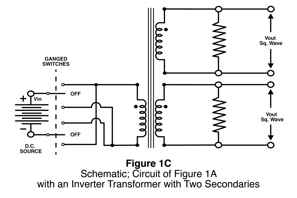
The inverter schematic of Figure 1C adds an electronic transformer inverter with two secondary windings. The switching action sends alternating current through the inverter transformer’s primary winding. This is referred to as push-pull action. The core has bipolar utilization. Bipolar utilization is discussed further below. The inverter transformer’s turns ratio can permit either higher or lower load voltage. The inverter transformer’s output is an A.C. square wave. Output filter networks can be used to obtain sine wave output. The inverter transformer can also provide electrical isolation between the inverter transformer’s input and output sides. Full wave rectification can be applied to the inverter transformer’s outputs to obtain a D.C. voltage of different value than that of the input source. This is shown in the schematic of Figure 1D.
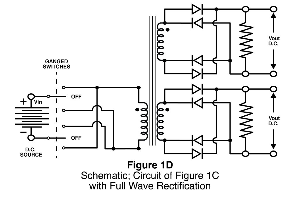
Compare the schematic of Figure 2A to the one in Figure 1D. Note in Figure 2A the center-tap connections on the electronic transformer windings, a set of two switches instead of a set of four switches on the input side, the two diodes on the secondary instead of four, and the output filter inductor between the capacitor and load.


The inverter transformer center-taps allow use of fewer switches and diodes. The inductors smooth out the current surges from the rectification thereby maintaining tighter output voltage regulation (less ripple voltage). The circuit in Figures 2A depicts a typical Push-Pull Forward Converter circuit. Be aware that the name for a Forward Converter circuit (and transformer) varies from industry to industry and from person to person. It may also be referred to as Buck, inverter, D.C. converter, feed forward, and others. There are also unipolar versions and there are bipolar versions that utilize saturable transformers to trigger transistor switching.
The Difference between Bipolar and Unipolar Applications
Since the connections of the electronic transformer “inverter” are alternated, the current direction through the electronic transformer will also alternate. Consequently the magnetic field polarity of the inverter transformer’s core will alternate between positive and negative flux directions. This is known as bipolar utilization of the inverter transformer’s core. This is graphically illustrated in Figure 2B. The B-H curve shown is also known as a hysteresis loop. The area inside the loop is related to the core loss.A thinner loop means less core loss.Also note the residual flux density point. In a unipolar application the flux density, B, would never return to zero value. It would stop at Br when the current (hence also the magnetizing force, H) returns to zero. The applied voltage reversal (by switching action) ensures that the flux density returns to zero. Bipolar utilization permits use of a smaller core than unipolar utilization because it permits a larger change in the core’s flux density. Fewer turns are needed to handle the same amount of power. Compare Figure 2B to Figures 3C, 4C, and 5C.
Unipolar utilization occurs if the magnetic flux remains in one direction. The value may vary up and down but does not cross zero value. A unipolar application is illustrated in Figures 3A, 3B, and 3C.
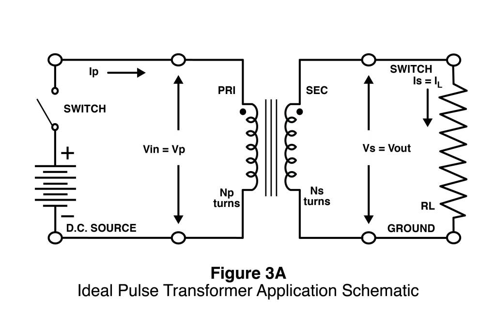


Some designers may refer to the transformer in Figure 3A as an inverter transformer, but it is not. It is serving as a pulse transformer with a resistive load. If we assume it to be an ideal transformer, then there is no core loss, no leakage inductance, it does not store any energy, and the residual flux density is zero. Figure 3B shows the expected output if a rectangular voltage pulse is placed across the transformer (turn switch on, then off). The output will also be a rectangular pulse without any distortion. There will be a change in amplitude because of the transformer’s turns ratio. The ideal transformer’s lack of stored energy eliminates the possibility of an inductive kickback voltage spike. This circuit does not produce an A.C. output, hence no true inverter action.
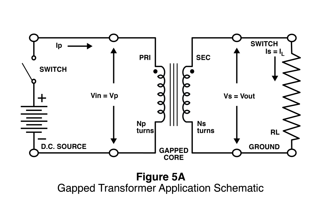
A non-ideal electronic transformer has finite inductance hence it stores some inductive energy in its magnetic field. A lower inductance results in more stored energy. Consider the non-ideal gapped transformer in the circuit shown in
Figure 4A.
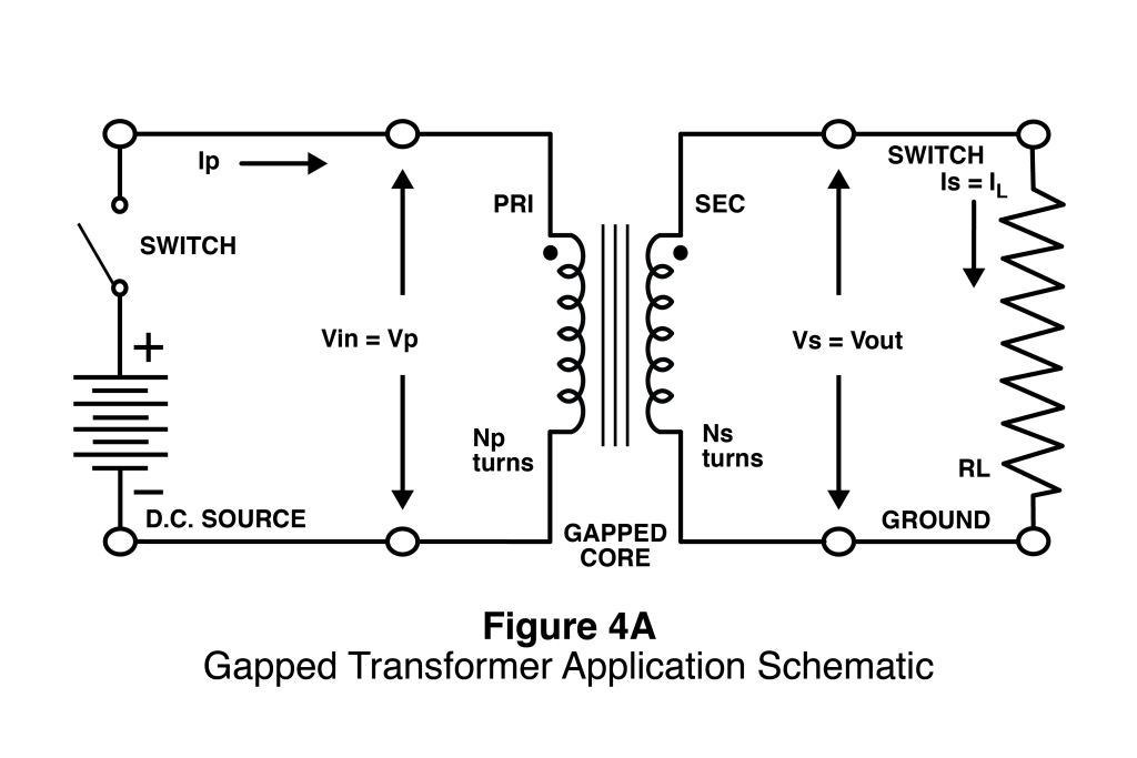


The gap lowers the inductance of the transformer; consequently more current can flow when the switch is closed (compared to no gap). When the switch is closed the transformer directly couples power to the load plus it stores energy in its magnetic field. The field is created by the magnetizing current. The current flow due to the load does not contribute to the stored energy. When the switch is opened the magnetic field collapses. The collapse creates an inductive kickback voltage of reversed polarity. The induced secondary voltage causes current to flow through the load resistor in the reversed direction. (This is how a flyback transformer functions.) The load sees alternating current although it usually has an asymmetrical waveform. One could claim that the circuits and transformer have inverter action.
The energy stored in the electronic transformer’s magnetic field is dissipated as heat produced by current flowing through the load resistor. Current of declining value will continue to flow until either all of the stored energy is dissipated or the switch is closed again. If completely dissipated, then the output shown in Figure 4B and the generalized hysteresis loop of Figure 4C apply. The transformer is said to be operating in discontinuous mode. The load voltage and load current reach zero value, and the core’s flux density reaches its residual value. Note that the flux density averaged over time is greater than zero. This holds for all unipolar applications. If the switch is closed again before all the energy is dissipated, then the output shown in Figure 5B and the generalized hysteresis curve of Figure 5C applies. The transformer is said to be operating in the continuous mode. The load voltage and load current remain above zero value, and the flux density does not reach its residual value. The output waveform in Figure 5B is more rectangular than that of Figure 4B.


The circuits in Figures 4A and 5A are not very practical inverter transformer circuits. To be useful the transformer must store as much energy as it directly couples to its load. Consequently, the transformer will tend to be lightly loaded and designed to have appreciable magnetizing current. Output filters would be required to produce a more symmetrical output waveform. These circuits find little use as shown here. There are D.C. biased unipolar applications, which function as inverters. They are not discussed here.
Saturable Transformers as Inverter Transformers
Figure 6A shows a Royer Inverter Circuit schematic that uses saturable transformers. The saturable transformer also functions as the inverter transformer. Figure 6B shows a Jensen Circuit which uses a saturable transformer and a power transformer.


The power transformer functions as the inverter transformer. Both of these circuits make use of push-pull switching to achieve the inverter action. The feature of these two circuits is the transistor switching action that is activated by a voltage spike created when the saturable transformer enters saturation. An oscillation develops which maintains the necessary switching action.
Quick Menu
Questions or Concerns?